
The High Cost of AI: Why HBM Memory Is Driving Up Prices
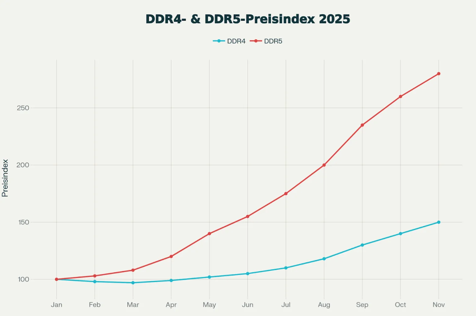
You've probably noticed it. That graphics card you've been eyeing? Suddenly way more expensive. The RAM for your PC? Not cheap. A big part of the reason why memory prices are crazy high right now isn't just about demand for your everyday gaming rig. It's about the insatiable appetite of artificial intelligence.
At the heart of this AI boom is a specialized type of memory called High Bandwidth Memory, or HBM. It's not what you find in your average PC. Instead, it's a critical component in the high-powered GPUs that drive AI development, and its unique, complex manufacturing process is directly impacting the cost of all memory.
So, what exactly is HBM, how is it made, and why is it causing such a stir in the market? Let's break it down.
What is Bandwidth, Anyway?
First off, "high bandwidth" isn't just marketing jargon. Bandwidth refers to how quickly data can be moved between components. Think of it like a highway: a wider highway with more lanes (bus width) and a higher speed limit (frequency) allows more cars (data) to travel at once.
Traditionally, GPUs have used GDDR memory. A high-end gaming card like the RTX 5090 might use 16 GDDR7 chips, each with a 32-bit bus width, totaling a respectable 512 bits. That's plenty for gaming.
But AI processing is on a whole different scale. NVIDIA's GB300 AI system, for example, uses four GPUs, and each is surrounded by eight HBM3E memory stacks. Each of these stacks boasts a massive 1024-bit bus width. Add it all up, and you get a staggering 8192-bit total bus width per GPU. That's more than 15 times wider than the gaming card's bus.
Simply cranking up the frequency on memory chips causes problems. Faster signal changes generate more electrical noise and hit physical limits on how quickly voltages can switch. So, HBM's solution? Go incredibly wide with the bus.
The Challenge: Fitting More Connections
All those extra wires needed for a wider bus create a space problem. A single GDDR7 chip might have around 266 connection points. An HBM stack, with its 1024-bit data bus alone, needs over 1000 connection lines, pushing the total to nearly 4000 points for all its functions.
How do you cram thousands of connections into a small footprint? It starts with how memory is traditionally packaged.
Traditional Memory Packaging
Normally, a delicate silicon chip (the "die") with tiny contact points is placed face-down onto a larger, more robust "substrate." This substrate, often made of glass fiber and epoxy resin, acts as a buffer. It contains its own layers of wiring to route the tiny contacts from the chip to larger solder points on the back, making it easier to attach to a circuit board.
But this traditional approach has limits. The rough surface of the glass fiber means circuit lines can't be packed too densely. Tiny air bubbles can get trapped during manufacturing, and the etching process used to create circuits can eat away at the sides of thin lines, making them fragile. For the thousands of connections HBM requires, this just won't cut it.
Enter the Silicon Interposer
HBM's solution is to ditch the glass fiber substrate for a silicon interposer. Imagine a perfectly flat, mirror-like piece of silicon—essentially a chip without transistors. Its ultra-smooth surface allows for incredibly fine metal lines, sometimes less than a micrometer wide, compared to the 10-micrometer-plus lines on traditional substrates. This allows for dramatically more connections in the same space.
The HBM chips and the GPU can be soldered directly onto this silicon interposer, connecting through its dense network of internal circuits. This solves the density problem and enables the wide bus needed for high bandwidth.
The Need for Capacity: Stacking Memory Dies
High bandwidth is crucial, but AI also demands sheer volume – capacity. A single GDDR7 chip might hold 2 gigabytes. Even 16 of them on a gaming card only reach 32 gigabytes. AI models need much, much more.
HBM achieves this through 3D stacking. Instead of laying memory chips side-by-side, multiple bare memory dies are stacked directly on top of each other. They all connect down through the silicon interposer. This dramatically increases the memory capacity without taking up significantly more board space.
Through-Silicon Vias (TSVs): The Vertical Highway
But how does the data get from the top chip all the way down through multiple layers to the interposer? Pulling wires out the side of every chip isn't feasible due to the sheer number of connections required.
The answer is Through-Silicon Vias, or TSVs. These are microscopic vertical holes drilled through the silicon dies and filled with copper. Each memory chip connects to these TSVs, creating a direct vertical pathway for data to travel down to the interposer.
Creating these TSVs is a marvel of engineering. It involves a precise etching process (like the Bosch process) to create the deep, narrow holes, followed by meticulous layering. First, an insulating silicon dioxide layer is applied to the inside walls, then a barrier layer (often tantalum or tantalum nitride) to prevent copper migration, and finally, copper is electroplated to fill the holes. After the wafer is thinned from the back, these copper columns create the electrical connections between stacked layers.
Microbumps and Assembly
On top of these copper TSVs, tiny copper pillars called microbumps are formed. These microbumps are then coated with a thin layer of tin. When the memory dies are stacked and heated, the tin melts, soldering the layers together.
This stack of thin, fragile dies, held together by these microbumps, is incredibly delicate. To provide structural support, companies fill the gaps between the dies. SK hynix, a leading HBM manufacturer, heats and solders the entire stack at once before molding it with epoxy resin. Samsung and Micron use a different approach, applying a polymer film between each die that melts and solidifies during the stacking process.
SK hynix’s method is generally considered faster and yields higher results because it solidifies the entire stack simultaneously with fewer intermediate materials. However, managing heat in these dense stacks is a major challenge. Companies like SK hynix incorporate additional TSVs purely for heat dissipation and use heat-conductive materials in their epoxy to improve thermal performance.
The AI Server Node: A Glimpse of the Future
The result of all this advanced manufacturing is staggering. In an AI server node like the NVIDIA GB300, each HBM3E stack can contain 12 memory layers, holding 36 gigabytes apiece. With eight stacks per GPU and four GPUs per node, you get over 1152 gigabytes—more than a terabyte—of memory in a single unit that can cost upwards of $300,000.
The next generation, HBM4, promises even greater density with a 2048-bit bus width and up to 16 memory layers. Future iterations might even move beyond microbumps to hybrid bonding, where polished copper surfaces are pressed directly together, allowing for even closer packing and better heat dissipation.
Why Memory Prices Are Crazy High: The Ripple Effect
So, how does this specialized, high-cost memory affect the prices we see for everyday components? It comes down to manufacturing capacity.
The complex processes and specialized equipment required to produce HBM—like advanced lithography, etching, and TSV fabrication—are also used for manufacturing standard DRAM and NAND flash memory. When chipmakers like SK hynix, Samsung, and Micron allocate more of their production lines and resources to churning out HBM for the booming AI market, there's simply less capacity available for traditional memory chips.
This reduced supply for regular DRAM and NAND means fewer components for graphics cards, SSDs, and other consumer electronics. Basic economics then dictates that with less supply and high demand, prices inevitably climb. So, the next time you wince at a memory price tag, remember that the cutting edge of AI is a significant factor driving that cost.
The Verdict
HBM is a technological marvel, essential for the continued advancement of AI. Its intricate design, leveraging silicon interposers, 3D stacking, and TSVs, pushes the boundaries of semiconductor manufacturing. However, this complexity, coupled with the intense demand from the AI sector, directly squeezes the production capacity for standard memory. This scarcity is a primary driver behind why memory prices remain stubbornly high across the board.
Comments
No comments yet — be the first to comment.